>>
Technology>>
Science and technology>>
Pioneering the Era of Photonic...Pioneering the Era of Photonic Quantum: A Photonic Quantum Chip Material Emitting 2 nm X-Ray Shortwaves

The Silicon Review
09 December, 2025
Author:
The Silicon Review Team
Inventor: Dr. Ko-Cheng Fang, CEO of LongServing Technology Co., Ltd
From Max Planck’s proposal of energy quantization to the discoveries of quantum dots (2023 Nobel Prize in Chemistry) and circuit quantum tunneling (2025 Nobel Prize in Physics), each breakthrough in quantum technology has reshaped humanity’s understanding of light and matter. Continuing this path of scientific innovation, Dr. Ko-Cheng Fang has developed a “2 nm photonic quantum material” that overcomes the physical limits of current electronic chip miniaturization and enables revolutionary photonic computing. This unprecedented new material’s core breakthrough lies in its ability to shorten light wavelengths to an average of 2 nm, entering the X-ray shortwave range, and thus it is named “X-Photon.”
The scale of the 2 nm photonic quantum material far surpasses the physical limits of existing materials, successfully overcoming the key barrier for replacing copper wires with photonic computation. The X-Photon material exhibits photon conduction, appears transparent when coated on the substrate, and is invisible to the naked eye. Its extremely tiny 2 nm structure cannot even be observed by a standard electron microscope. When tested with three different laser colors (red, green, and blue), the X-Photon material produces visible white light points corresponding to its 2 nm photon wavelength. Further analysis using Raman spectroscopy and X-ray diffraction confirms that this material is unknown in nature, demonstrating its originality and rarity.
Currently, advanced semiconductor processes rely on copper wires for electronic signal transmission, with line widths around 14 nm. Although silicon photonics is actively being developed, mainstream materials such as indium phosphide (InP) face severe wavelength limitations, operating around 1310 nm to 1550 nm, primarily for data transmission, and cannot replace nanoscale copper wires for core computation. Quantum dot materials, with wavelengths between 300 nm and 700 nm, are applied in display technologies but likewise cannot meet the requirements of advanced semiconductor processes.
Today, Dr. Fang has created the 2 nm photonic quantum material—a breakthrough that transcends the limits of nature, redefining wavelength scales and the rules of light physics. This is no longer merely an engineering optimization but a fundamental innovation shaking the foundations of physics. The significance of the 2 nm photonic quantum material is that computing technology can, for the first time, break free from the electronic world. Humanity is entering a wholly new photonic quantum era, possessing not only technical breakthroughs but also scientific weight and global impact at a Nobel-level scale. What it opens is not just a new path for chip development but a future avenue capable of redefining technology, industry, and civilization itself.
A Historical Review of Quantum Mechanics — From Planck to the Dawn of the Photonic Quantum Era
Quantum mechanics began in the early 20th century as scientists sought to explain phenomena that classical physics could not, such as blackbody radiation and atomic spectra. In 1900, Max Planck proposed the concept of “energy quantization,” planting the seed of a scientific revolution. Physicists including Einstein, Bohr, and Heisenberg later built the framework of quantum theory, fundamentally reshaping our intuitive understanding of the physical world. From wave–particle duality to the uncertainty principle, quantum theory has become the foundation of modern technology and has driven multiple groundbreaking applications.
Quantum Dots — A Revolution in Wavelength Optics
Quantum dots are semiconductor crystals whose core mechanism is the “quantum confinement effect”: when a material shrinks to extremely small dimensions, its electronic energy levels become discrete. By adjusting the particle size, scientists can precisely control the bandgap and thereby tune the color of the light emitted by the quantum dots. This technology saw breakthroughs in the 1980s, followed by stable synthesis methods in the 1990s, and received recognition with the 2023 Nobel Prize in Chemistry (Fig. 1).
-
Laureates: Moungi G. Bawendi, Louis E. Brus, and Alexei I. Ekimov.
-
Applications: Modern QLED television displays, LED lighting, biological labeling, and medical imaging (Fig. 2).
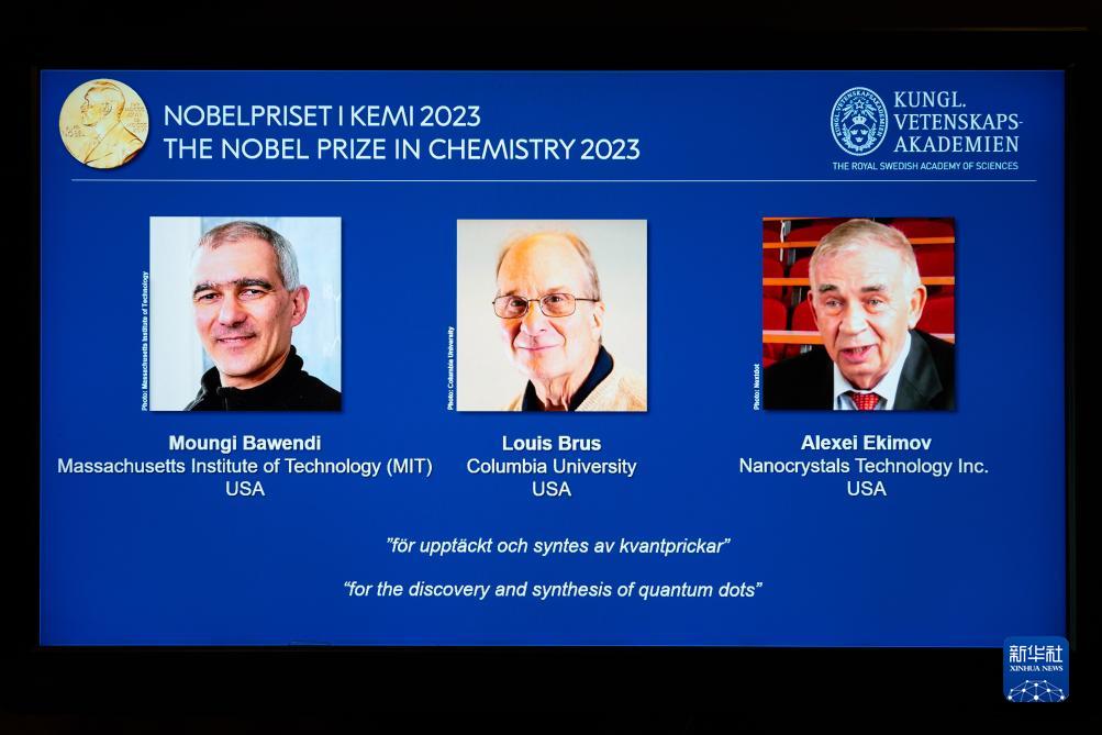
Fig. 1. Moungi Bawendi, Louis Brus, and Alexei Ekimov receive the 2023 Nobel Prize in Chemistry for their work on quantum dots [1].

Fig. 2. Quantum dot materials [2]
Quantum Tunneling — The Electron Revolution
Quantum tunneling is a counterintuitive yet essential phenomenon in quantum mechanics: microscopic particles have a certain probability of passing through potential barriers that are insurmountable under classical physics. This effect is at the core of the modern semiconductor revolution and is widely applied in electronic components such as flash memory. Although the theory was proposed as early as 1928 by George Gamow and others, the research that achieved its macroscopic realization and verification was recognized with the 2025 Nobel Prize (Fig. 3).
-
Laureates: John Clarke, Michel H. Devoret, and John M. Martinis.
-
Applications: Quantum computers, quantum sensors, and quantum cryptography.
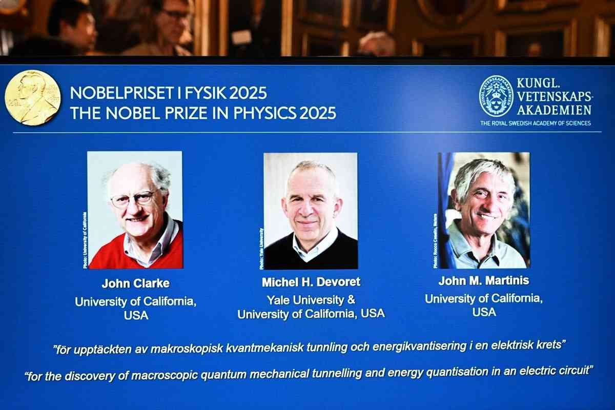
Fig. 3. John Clarke, Michel H. Devoret, and John M. Martinis receive the 2025 Nobel Prize in Physics for the discovery of macroscopic quantum mechanical
tunnelling and energy quantisation in an electric circuit [3].
The Inventor Who Broke the Nanoscale Limit and Redefined the Physics of Light
Dr. Ko-Cheng Fang (Fig. 4) — The first in human history to create a 2 nm wavelength material. “When quantum dots rewrote optics and quantum
tunneling rewrote electronic behavior, the 2 nm photonic quantum material rewrites the fundamental limits of material properties at the nanoscale.”

Fig. 4. Dr. Ko-Cheng Fang, CEO of LongServing Technology. (Courtesy of LongServing)
The 2 nm scale is not merely a miniaturization—it is a breakthrough of physical boundaries. This innovative invention directly challenges Nobel-level science. Its core technology shortens the photon channel wavelength to an average of 2 nm, representing the physical limits known to humanity—or what was previously thought impossible. Even the most advanced extreme ultraviolet (EUV) light has a wavelength of 13.5 nm in vacuum. Therefore, the creation of this material is unquestionably a Nobel-caliber achievement, capable of advancing human civilization by more than a century.
What Materials in the World Can Emit 2 nm Wavelengths? The answer lies in wave–particle duality—a type of matter wave, such as moving particles like electrons. Copper, being the best conductor, can generate electrons. Therefore, to replace copper, a material must be an invention that breaks the physical limits.
When Dr. Fang set out to develop a photonic computing chip to replace copper as the basis for photonic computation, he had already thoroughly studied silicon photonics and quantum dot materials. Both, however, have wavelengths that are far too long. In fact, no material in the world naturally exists with such a short wavelength. This led Dr. Fang to develop the photonic quantum material. By contrast, Taiwan’s national silicon photonics initiative, bringing together dozens of major technology companies including TSMC, focuses on silicon photonics using wavelengths of 1310 nm and 1550 nm for data transmission. Yet, this approach still cannot replace 14 nm copper wires.
To fully replace electronic chips for photonic computation, the photosensitive material must have a wavelength comparable to that of electronic materials. In current advanced semiconductor processes, copper wires are buried with line widths of about 14 nm. Therefore, the key challenge was to develop a material that is not only photosensitive but can also shorten the wavelength to at least below 10 nm in order to replace copper wires. This represented the greatest difficulty and challenge in the entire research process.
Happily, Dr. Fang succeeded in creating a new material that shortens the wavelength to an average of 2 nm—already in the X-ray shortwave range. For this reason, it was named the “X-Photon.” Using Raman spectroscopy and X-ray diffraction (see Appendix II for detailed analysis), the crystal structure of this photonic quantum material could not be identified, demonstrating that it is an unknown material in nature and can be considered a completely unprecedented type of material.
In the world, there is no material that cannot be detected by instruments, especially when using Raman spectroscopy to measure wavelength and X-ray diffraction to analyze crystal structure—techniques capable of atomic-level detection. Yet even with these methods, the exact composition of this X-Photon material could not be determined. While similar materials exist, none could be analyzed successfully; even rare earth elements can be easily detected. This highlights the extraordinary significance of Dr. Fang’s invention.
Silicon Photonics and Quantum Dots: The Material Bottlenecks of Modern Technology
Indium phosphide (InP) is used in silicon photonics. Being a phosphide compound, it is inherently photosensitive and can emit light. However, its wavelength is above 1000 nm, making it suitable for photonic applications on silicon platforms primarily for data transmission [4]. InP also has a higher electron mobility than commonly used silicon or gallium arsenide semiconductors, making it applicable for high-power, high-frequency electronic circuits. Due to its direct bandgap, InP is ideal for optoelectronic devices such as laser diodes and serves as an epitaxial substrate in InGaAs-based optoelectronic components.
Quantum dot (QD) materials have wavelengths between 300 nm and 700 nm, which are unsuitable for semiconductor chip applications. Their main use is in quantum dot displays for improving resolution. Quantum dots are nanoscale semiconductor particles whose optoelectronic properties, such as emitted light color, depend on particle size and can be precisely tuned by adjusting their dimensions. Common materials include cadmium selenide (CdSe), cadmium sulfide (CdS), indium arsenide (InAs), or cadmium-free perovskites. Quantum dots have a wide range of applications, including displays (e.g., QLED TVs), lighting, solar cells, biological labeling, and medical imaging.
X-Photonic Materials: A Revolution Breaking the Limits of Modern Materials
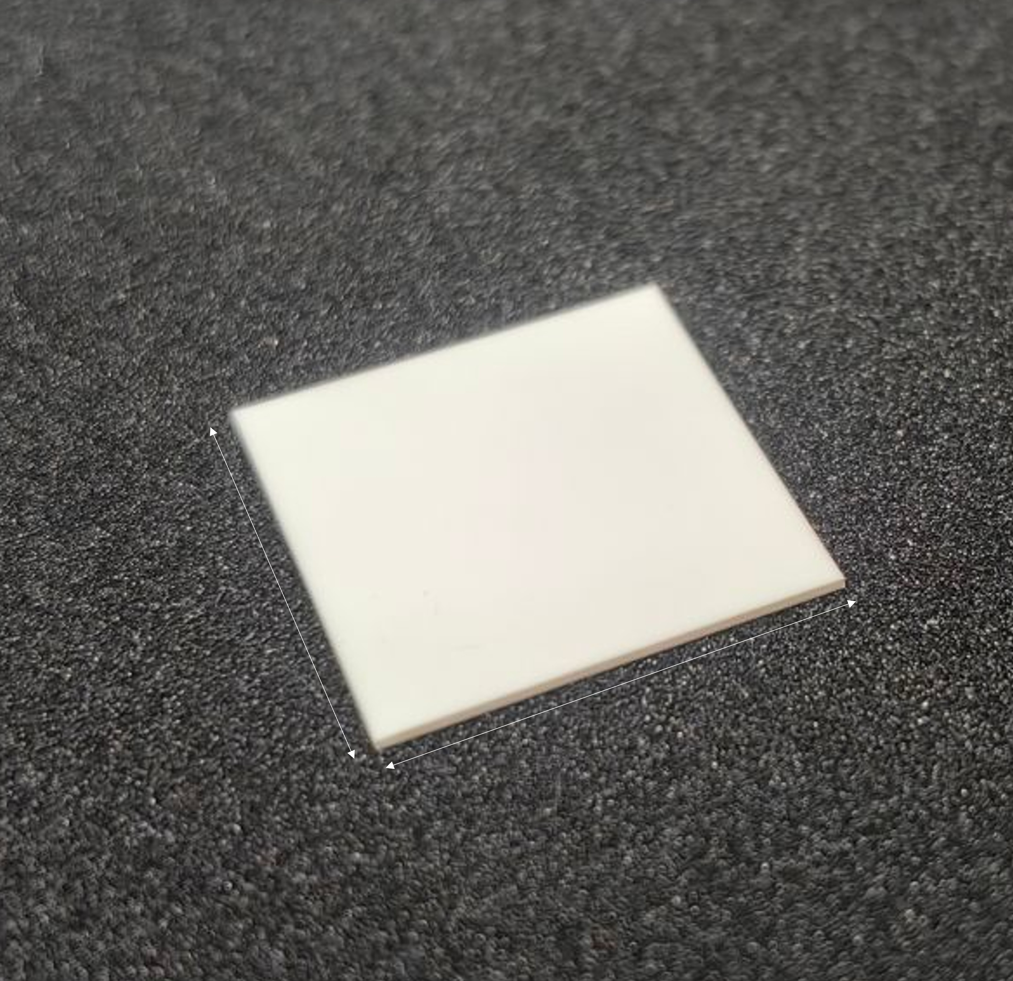
Dr. Fang’s X-Photon materials fundamentally rewrite physical laws, exhibiting exceptional photon conduction capabilities at different scales under laser excitation. When a photonic chip is coated with X-Photon material on a ceramic substrate, it appears transparent, a property unattainable by conventional materials. The key behind this lies in Dr. Fang’s development of 2 nm-scale photonic quantum material.
At such an extremely small scale, the material is completely invisible to the naked eye in the visible light range (Fig. 5). Furthermore, even standard electron microscopes cannot resolve the 2 nm photonic circuitry; the resulting images appear as an overall gray-black area (Fig. 6).
The ability to maintain stable and controllable optical waveguide behavior at such a microscopic scale represents a major breakthrough. This advancement not only marks a significant leap in materials science and photonic engineering but also demonstrates the material’s key value and revolutionary potential for future photonic chips, quantum optics, and advanced optical communication technologies.
|
Fig. 5. Ceramic substrate coated with X-Photon material. (Courtesy of LongServing) |
Fig. 6. Electron microscope image of 2 nm photonic material. (Courtesy of LongServing) |

Spectral Visibility of X-Photon Materials
Visible light refers to the range of electromagnetic waves perceptible by the human eye. Although individual sensitivity may vary slightly, the generally accepted wavelength range is approximately 380 nm to 780 nm, with the human eye being most sensitive to the yellow-green region in the middle of the spectrum. Wavelengths shorter than violet light are called ultraviolet (UV), while wavelengths longer than red light are called infrared (IR). Both UV and IR belong to the invisible light range (Fig. 7).
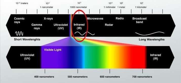
Fig. 7. Electromagnetic spectrum of visible light [5].
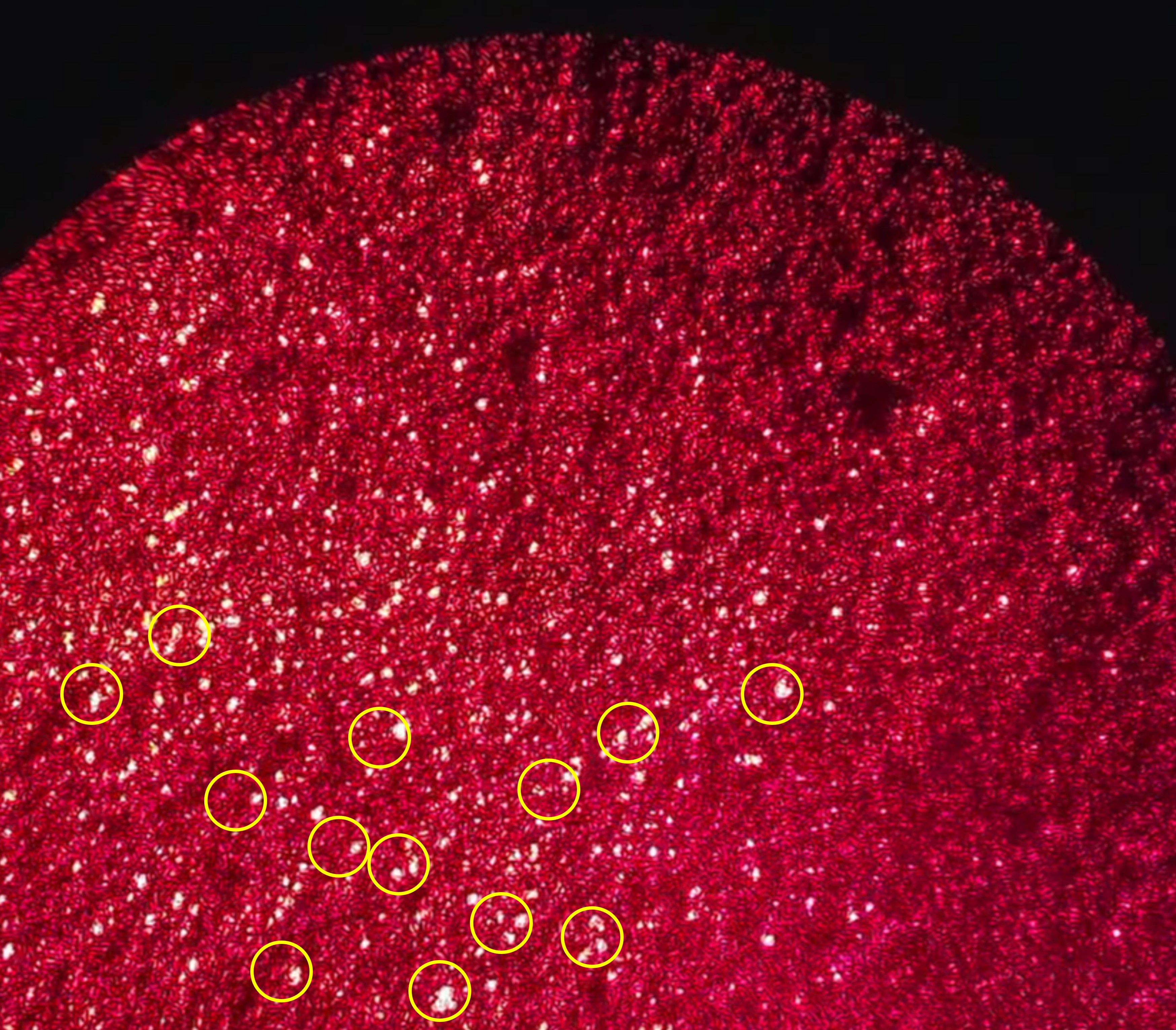
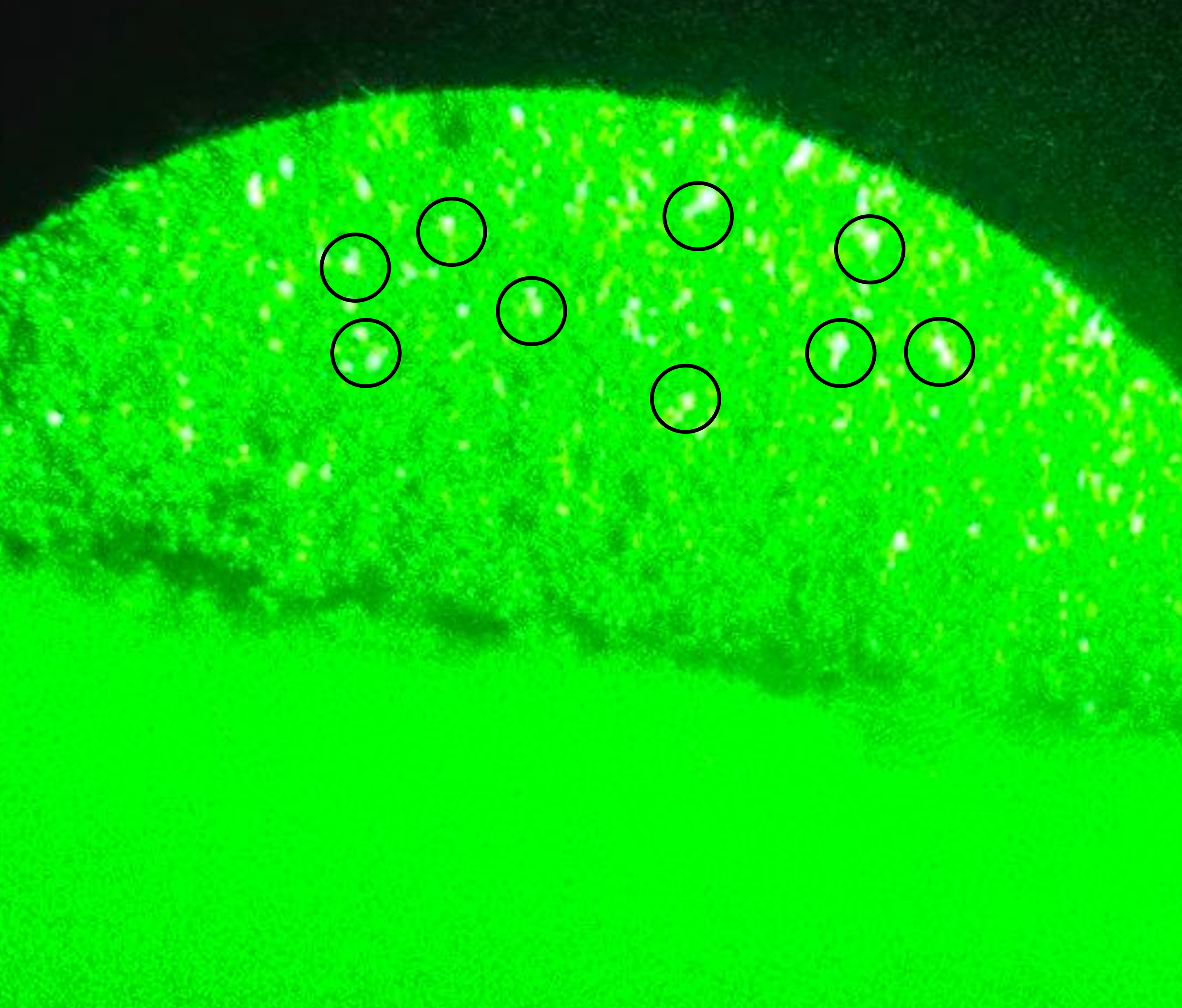
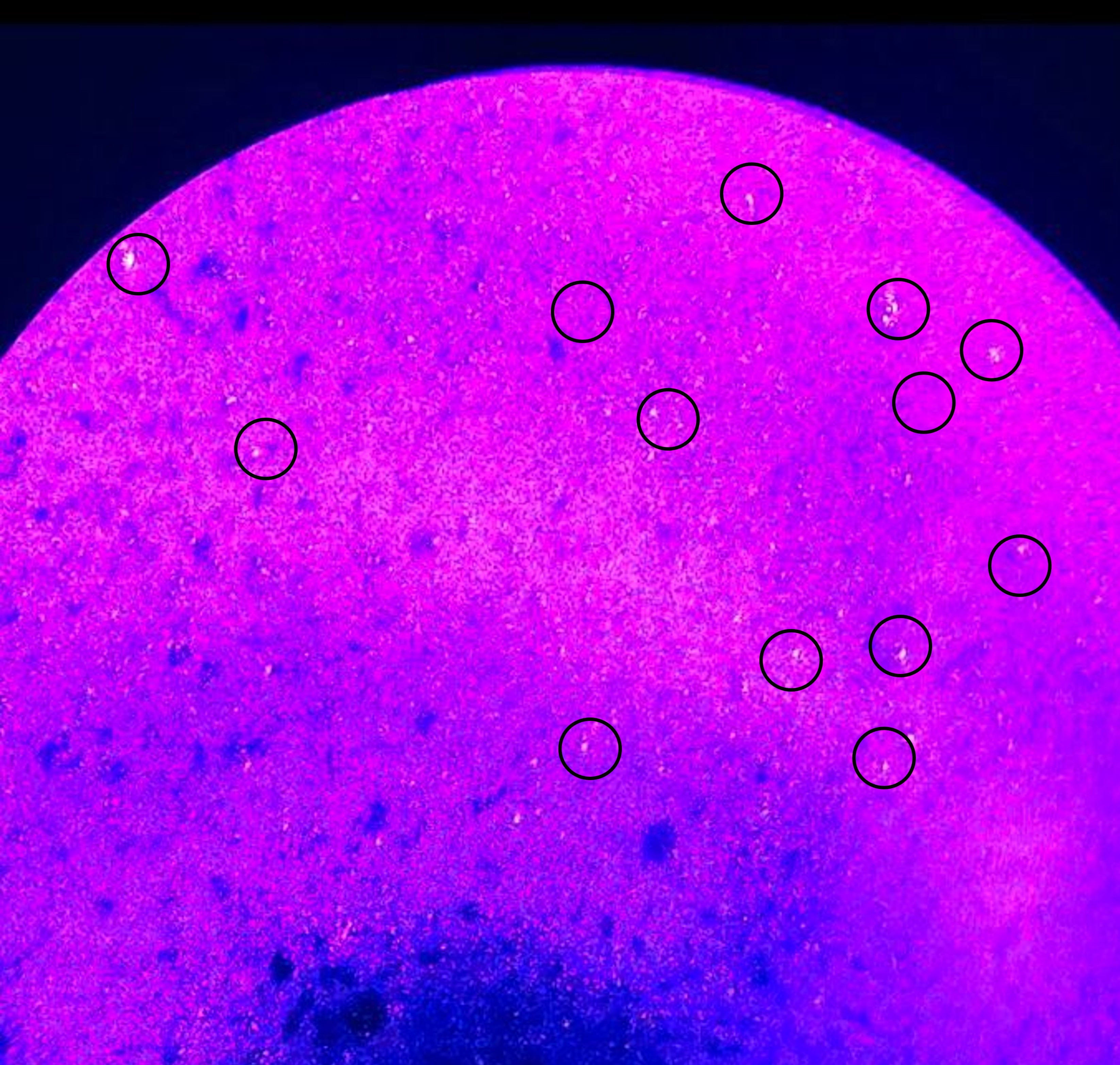
Tests were conducted using three different laser colors: red, green, and violet-blue. The results showed that under illumination from any of these lasers, the photonic material exhibits a photon wavelength of 2 nm, which is completely invisible to the naked eye. Therefore, regardless of the laser color used, the material does not reflect the color of the incident laser.
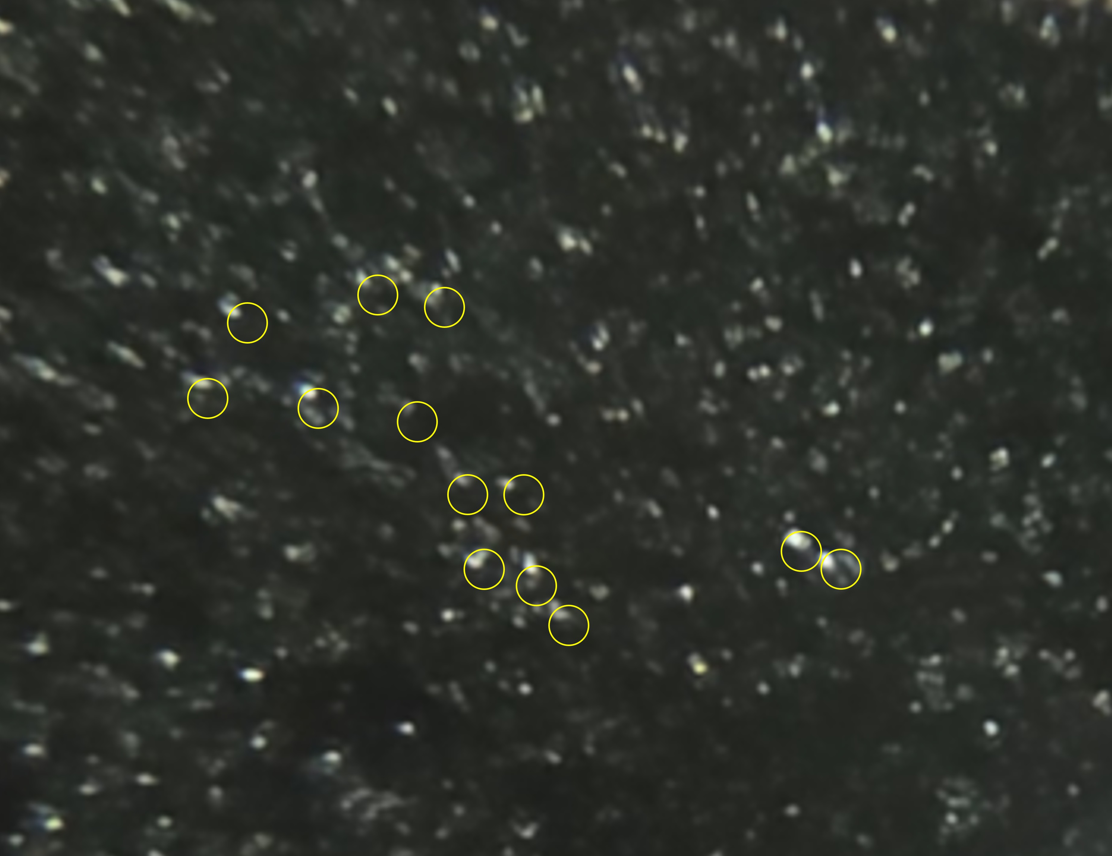
So, what color does it appear as? In fact, it manifests as white light (indicated by circles). This phenomenon can be clearly observed at the circled positions in Figures 8–10. Additionally, this photonic material is capable of emitting ultrashort waves similar to X-rays, with wavelengths ranging from 0.01 nm to 10 nm.
|
|
|
|
|
Fig. 8. X-Photon material under red laser illumination.(Courtesy of LongServing) |
Fig. 9. X-Photon material under green laser illumination.(Courtesy of LongServing) |
Fig. 10. X-Photon material under violet-blue laser illumination.(Courtesy of LongServing) |
X-Photon Material for Copper-Free Photonic Chip Technology
Using ultra-high-resolution electron microscopy (30 kV accelerating voltage with 3.13 pA current), the photonic chip was observed inside a vacuum chamber. Due to the vacuum environment, the X-Photon material could not be exposed to light during observation. Therefore, the material was examined under averaged coating conditions.
As shown in Fig. 11, distinct white light spots (indicated by circles) can be clearly observed, representing the characteristic average 2 nm photon wavelength. This X-Photon material is expected to be widely applied in photonic chips in the future, replacing copper wires used in conventional electronic chips.
|
|
|
Fig. 11. White light spots (indicated by circles) correspond to photons with a 2 nm wavelength.(Courtesy of LongServing) |
Three Major Breakthroughs of the Photonic Quantum Chip
In developing the photonic quantum chip, Dr. Fang focused on material science and chemical processing rather than relying on expensive physical equipment. The greatest challenge was not manufacturing the chip itself, but how to overcome the material limitations. While conventional electronics can operate at 14 nm line widths, quantum dot materials, with wavelengths between 300–700 nm, are simply too large for practical chip applications. Dr. Fang’s X-Photon material, however, achieved three seemingly impossible breakthroughs:
1.Wavelength reduced from 1300 nm to 2 nm (X-ray wavelength)
With the development of X-Photon material, the wavelength of silicon photonics was reduced from 1300 nm directly to an average 2 nm, reaching the X-ray photon range — a monumental achievement in human history.
2. 2 nm photonic quantum pathways
The 2 nm photonic quantum material is not just an improvement; it rewrites the laws of physics. This represents the known physical limit for humans and is a material absent in nature. Even if someone knew its composition, it could not be reverse-engineered, because such a structure does not occur naturally.
3. Mass Production of Photonic Chips Using Medical-Grade X-Rays — No EUV Lithography Required
From the beginning, Dr. Fang designed the photonic quantum chip to bypass EUV lithography. He further simplified the manufacturing process, eliminating the need for complex photolithography, etching, deposition, or copper wiring, and instead created direct photonic pathways. The core technology is illustrated in Fig. 12. This marks the first time in human chip history that a chip design completely bypasses traditional semiconductor fabrication. By simplifying the process and using medical-grade X-rays, the photonic chip can be manufactured without the need for conventional EUV lithography.
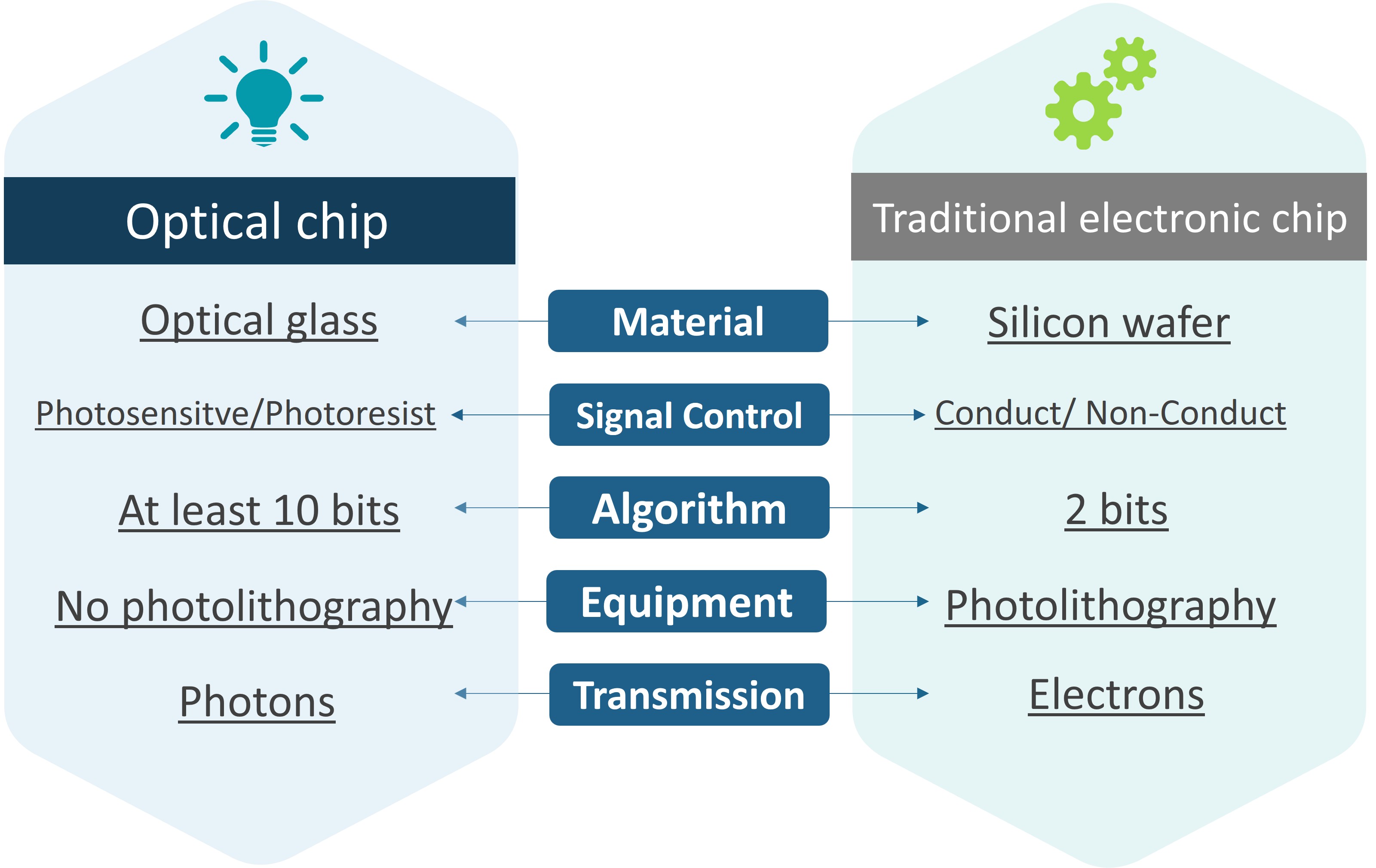
Fig. 12. Core technology of the photonic quantum chip. (Courtesy of LongServing)
In physics, X-rays have wavelengths roughly between 0.01 nm and 10 nm, while most medical applications use shorter-wavelength hard X-rays. Traditionally, X-rays were considered unsuitable for chip fabrication because conventional photoresists only respond to wavelengths in the 5–15 nm range, and producing usable wavelengths required national-scale facilities such as synchrotron radiation accelerators. These facilities are both expensive and incapable of supporting mass production.
However, these limitations were not an obstacle. Dr. Fang was able to independently develop and produce both photosensitive materials and photoresists, overcoming the dependency of traditional fabrication processes on specialized materials. He successfully applied medical-grade X-rays for the mass production of photonic quantum chips.
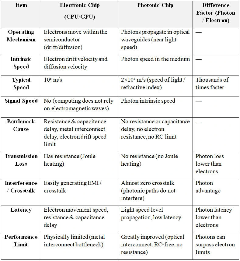
Dr. Fang also unveiled a 7 nm photomask (Fig. 13) with a development image captured via electron microscopy. This achievement surpasses all existing advanced photomask technologies, including those used by companies like TSMC, which remain at 28 nm. When comparing photonic quantum chips of the same class to existing electronic chips, the computational power of the photonic quantum chips is approximately 1,000 times higher (Table 1). It is evident that, once photonic quantum chips are commercialized, all existing semiconductor transistors may become obsolete, much like vacuum tubes, destined for museums.
When photonic quantum chips deliver thousands to tens of thousands of times more computing power, the sector most impacted could be cryptocurrencies. Digital currencies that rely on massive clusters of electronic mining rigs for wealth generation depend heavily on computational power for encryption and decryption. Once this computational barrier is surpassed, the entire cryptocurrency landscape could be fundamentally transformed.

Fig. 13. Electron microscope image of 7 nm photomask for the photonic chip.
(Courtesy of LongServing)
Table 1. Comparison of Physical Properties between Photonic and Electronic Chips
The End of Electronic Chips: The Limit of Moore’s Law
Electronic chips are constrained by Moore’s Law. As chips shrink to the nanometer scale, leakage and overflow issues become increasingly severe. Quantum tunneling effects cause the distinction between 0 and 1 signals to blur. IC engineers must rely on algorithms to interpret these signals, and with the extensive use of AI, power consumption continues to rise while performance declines. For example, a single data center can consume as much electricity as an entire town. This crisis is spreading across the entire technology sector. In Taiwan, for instance, there is a push to develop solar power to meet energy demands, but solar farms are environmentally challenging to recycle, and can cause severe losses after typhoons.
Photonic quantum chips represent the future of humanity. As Einstein once said, “Photons are quanta.” Nano-scale photonic chips are effectively quantum chips, where their signals are quantum signals. A photonic quantum device, such as a quantum smartphone, can seamlessly interface with existing electronic systems using standard 0 and 1 outputs. At the same time, it can output quantum bits, enabling entirely new computational methods. Such computing power is capable of meeting any AI requirements from today into the future.
AI Energy Crisis: The True Cost Behind the Computing Boom
Since NVIDIA’s graphical recognition systems became the optimal tool for AI, they directly fueled a massive boom in the technology sector on Wall Street. However, when concerns about an AI bubble arise, the first questions are always power consumption and investment costs.
Modern chip manufacturing is an extremely complex process. For example, a photomask for a 7 nm chip costs roughly 15 million USD, and a single extreme ultraviolet (EUV) lithography machine can cost hundreds of millions of USD[6]. Additionally, the complex supply chain requires national-level support — from photoresists from Japan to lenses from Germany — making it almost impossible for an individual or a single company to enter the chip manufacturing industry independently.
Consider NVIDIA’s H100 GPU, which consumes 700 W per card. An AI computing center with at least 800 cards would use a total of 5.6 MW, and when including the cooling systems, a single AI cluster can consume 10–15 MW, equivalent to the electricity usage of a small town. Scaling to thousands of AI clusters would require an astronomical investment, far beyond general comprehension.
This is why electronic AI falls into a “power-hungry black hole”: many AI clusters in the U.S. simply gather dust because infrastructure and power supply are insufficient to support them.
The Bottleneck of the Electronic Era: AI Investment Bubble and the Imminent Comeback of Photonic Technology
Dr. Fang remarked: “Time is running out for electronic chips. Their development has reached a bottleneck.” While Wall Street investors craft grand AI visions, building massive data centers that consume the Earth’s resources to support electronic AI, they fail to realize that investment costs often exceed returns.
For example, countless AI chips are used to train robots. Yet so far, whether for vacuum cleaning or cooking, the investment cost of AI robots is still higher than hiring a human worker. Meanwhile, the same funds could have been used to train numerous outstanding engineers.
This is the limitation of electronics: electronic computing is too slow. The human brain does not operate in 0s and 1s sequentially — it functions at the speed of light. Achieving this speed requires photonic chips and quantum computing, which can surpass and even replace human capabilities. Consider current supercomputers: they can beat humans in chess, but only because they rely on enormous databases and massive computing centers.
Such investment is inherently inefficient. Countries worldwide have poured vast amounts of capital into electronic chip manufacturing, pushing toward 2 nm technology. But even if chips reach 1 nm, how much faster will computing truly become? Is it worth the investment?
In contrast, photonic chips consume far less power and can achieve computing speeds thousands of times faster. With quantum computing, speeds could exceed ten thousand times those of conventional electronics. The gap in investment efficiency between photonic chips and electronic AI chips is staggering.
A looming crisis is forming: when it bursts, the photonic storm could sweep through the electronics industry, triggering widespread closures and eliminations, potentially dealing severe blows to technology stocks.
True Innovative Technology: Shaping the Next Twenty Years of the Tech Industry
If a technology’s research and development cannot guarantee returns over the next twenty years, companies are unlikely to invest. For example, today, one can outproduce an automaker, but tomorrow, another competitor can surpass you with even greater production. In such cases, all previous investments are wasted.
However, possessing a genuine technological innovation, particularly one protected by patents, can secure an enterprise’s investment for the next two decades. While most major tech companies hold thousands of patents, not all patents are truly strategic. Many R&D personnel pursue patents primarily for rewards, often modifying existing designs just to obtain one. Such patents are essentially a waste of resources.
Truly innovative technology can lead and dominate an entire sector. Take Dr. Fang’s photonic quantum computing chips as an example. While “photonic transmission” chips exist everywhere, none of them use photons for computation. Dr. Fang's photonic quantum chip is the only one that uses photonic computing; even Taiwan's semiconductor industry does not possess this technology.
When the world is reshaped by photonic quantum computing, every aspect of human life — from food to transportation — will be profoundly affected. Consider the 2 nm photonic coatings: their wavelength is so short that they are invisible to the human eye, granting exceptional stealth capabilities. In the laboratory, these coatings appear transparent, only visible under a laser in an electron microscope.
The potential applications are enormous. Whether in autonomous vehicles or aerospace, these materials will have a transformative impact. In the future, a landscape of technology will appear almost entirely glass-like, embedding countless photonic pathways. Photonic gates will be predictable and will fundamentally change the way humans perceive devices such as smartphones.
Conclusion
Looking back at the history of science, every discovery honored with a Nobel Prize is remembered not for its technical sophistication, but for permanently reshaping humanity’s understanding of nature:
-
Planck quantized energy, opening the door to the microscopic world.
-
Einstein explained the photoelectric effect with photons, sparking an optical revolution.
-
Quantum dots demonstrated that matter can control light based on size, reshaping display and materials technology.
-
Quantum tunneling turned previously insurmountable energy barriers into controllable phenomena, ushering in the era of quantum technology.
Today, Dr. Ko-Cheng Fang has created the 2 nm photonic quantum material, an invention that surpasses the limits of nature and redefines wavelength scales and light physics. By compressing light’s wavelength to 2 nm and forming stable photonic pathways at an unprecedented extreme scale, this breakthrough is not merely an engineering optimization, but a fundamental innovation that challenges the very foundations of physics.
As with historic achievements recognized by the Nobel Prize, the significance of 2 nm photonic quantum material is far beyond faster or more energy-efficient chips. It allows computing technology to break free from the electronic world and enter the realm of photons. Chips can now operate entirely with light rather than electrons, no longer constrained by copper wiring, EUV lithography, or nanoscale processes, but based entirely on new materials and a new physical dimension. This is a century-advancing technological milestone, rivaling quantum dots and quantum tunneling, and even surpassing the semiconductor revolution.
When all-photonic computing becomes reality, and 2 nm photonic pathways replace electronic conductors, the physical laws governing computing speed, energy consumption, and latency will be rewritten. Humanity will enter a completely new photonic-quantum era, marked not only by technological breakthroughs, but also by Nobel-level scientific significance and global impact. This innovation opens not just a new path for chips, but a future highway capable of redefining technology, industry, and civilization itself.
Appendix I. References
-
https://commons.wikimedia.org/w/index.php?curid=26950552
-
https://hk.epochtimes.com/news/2025-10-08/26102420#google_vignette3
-
https://www.lightuf.com/news/%E5%85%89%E7%9A%84%E5%A5%BD%E8%99%95/%E7%B4%85%E5%85%89-%E7%B4%85%E5%A4%96%E7%B7%9A-%E8%BF%91%E7%B4%85%E5%A4%96%E7%B7%9A-%E9%81%A0%E7%B4%85%E5%A4%96%E7%B7%9A-%E6%9C%89%E7%94%9A%E9%BA%BC%E9%97%9C%E4%BF%82%E5%97%8E.htm?srsltid=AfmBOoqq9qW4CiPzYYDWNwuAxWakEf7jVqfhp-RQfsYJX2XwJpDy4IwN
-
Ibtisam Abbasi, 2025.3.25, Are Photonic Chips Better than Silicon Chips? https://www.azooptics.com/Article.aspx?ArticleID=2757
-
Blake Crosley, Liquid Cooling vs Air: The 50kW GPU Rack Guide (2025) https://zh.introl.com/blog/liquid-cooling-gpu-data-centers-50kw-thermal-limits-guide
Appendix II. Raman Spectroscopy and X-ray Diffraction Analysis
The sample used in this analysis was provided by Dr. Yung-Chang Tu (Ph.D. in Civil and Geological Engineering) from National Pingtung University of Science and Technology, and analyzed at the laboratory of Prof. Jiann-Shing Lee, Department of Physics, National Pingtung University.
I Sample Description
1.Sample: Ceramic substrate coated with the photonic quantum material
2.Purpose: To investigate the characteristics of the photonic quantum material using Raman spectroscopy
II Raman Spectroscopy Analysis
1. Raman measurements were performed using a Raman spectrometer with the excitation laser set to a standard visible-light wavelength. The measurement range was 100–2000 cm⁻¹.
2.Peak positions observed at 167.6 and 205.5 cm⁻¹ do not match typical alumina ceramic substrate signals and are presumed to originate from the Raman response of the photonic quantum material coating itself.
3.Peak positions at 375.8, 414.7, 642.0, and 748.2 cm⁻¹ correspond to characteristic Raman peaks of α-Al₂O₃, representing the inherent signals of the alumina ceramic substrate.
4.Peak positions at 574.3, 659.8, 671.6, and 703.1 cm⁻¹ fall within regions associated with alumina and other oxide responses. These peaks are presumed to arise from the porous structure, surface defects, or secondary phases of the alumina ceramic substrate.
5.In the 1200–1800 cm⁻¹ region, the spectral baseline rises significantly with broad peak superposition, characteristic of strong fluorescence induced by laser excitation. This fluorescence effect suppresses or obscures potential Raman signals.
6.Conclusion of Raman Spectroscopy Analysis:
The spectrum clearly identifies the characteristic peaks of the alumina ceramic substrate and reveals additional peaks originating from the photonic quantum material. However, these peak positions do not correspond to known literature or existing material phases, and strong fluorescence interference limits further identification. Therefore, Raman spectroscopy in this test cannot determine the specific material type or chemical composition of the photonic quantum material. It can only confirm that the material is indeed present and produces observable effects on the overall spectrum.
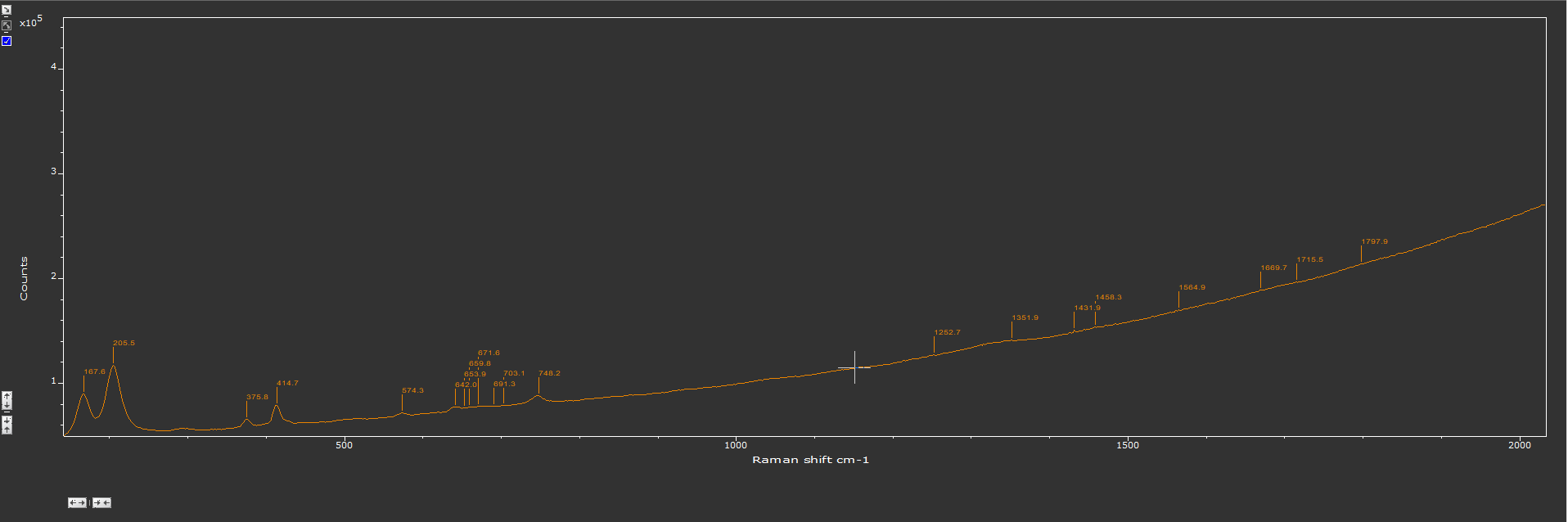
Fig. 1. Raman spectrum of the photonic quantum material.
-
X-ray Diffraction Analysis
-
Based on the XRD diffraction pattern of the photonic quantum material, strong peaks are observed in the regions of approximately 2θ = 25°–35°, 37°–43°, and 57°–67°, corresponding to common crystal planes of α-Al₂O₃ (such as (012), (104), (110), and (113)). Database comparison also confirms Al₂O₃ as a reasonable and primary matching phase, indicating that the characteristic peaks of the ceramic substrate are indeed present in the sample.
-
From the combined diffraction pattern and database comparison results, all identifiable major peaks originate from the ceramic substrate (Al₂O₃). The diffraction signals of the photonic quantum material coating are relatively weak, and their peak positions overlap with multiple possible phases, making it impossible to distinguish its composition, crystalline phase characteristics, or material properties using XRD.
-
Conclusion of X-ray Diffraction Analysis:
XRD cannot identify the composition or crystalline phase characteristics of the photonic quantum material, nor can it determine the elements present within the material.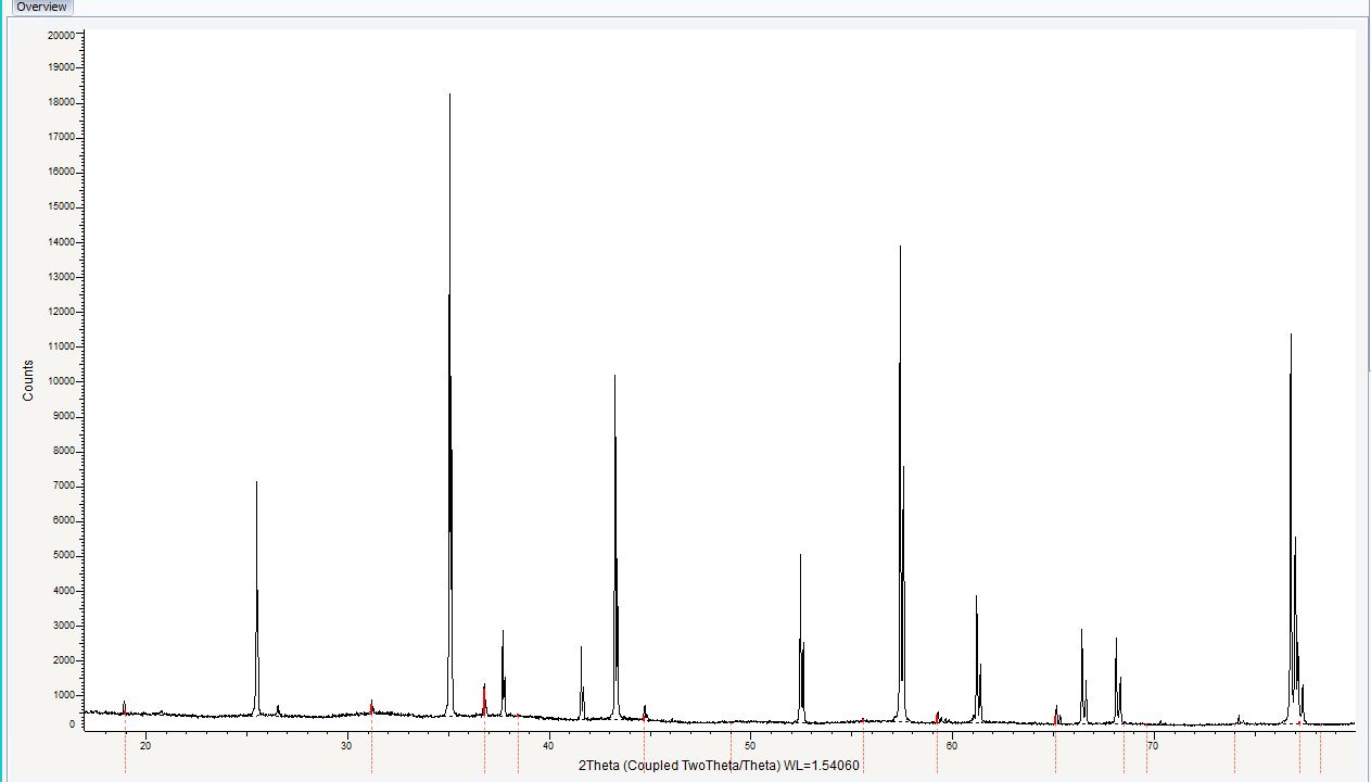
Fig. 2. XRD pattern of the photonic quantum material