30 Innovative Brands of the Year 2022
‘Our X-NAND Technology will Bring about a Revolution of Speed to the Entire Data Storage Industry’: Andy Hsu, CEO of NEO SEMICONDUCTOR
The Silicon Review
![]()
“X-NAND provides a perfect high-density, high-speed, and low-cost solution for the next generation of NAND flash memory products.”
NAND Flash is a type of non-volatile storage technology that does not require power to retain data. NAND Flash is all around us – in our smartphones, modern televisions, computers, tablets, and our homes and offices. Anything with artificial intelligence (AI) and needs to retain data is likely to contain NAND Flash. There is a new player in the NAND Flash market, 3D NAND. It is arguably the biggest NAND development since its inception.
NEO Semiconductor is one such company that is predominantly focusing on the next generation of 3D NAND flash memory technology. The company was founded in 2012 by Andy Hsu and a team in San Jose, California. The company currently owns 22 U.S. patents in-memory design architectures and cell structures. In 2018, the company made a breakthrough in 3D NAND architecture by introducing its cutting-edge product named X-NAND. X-NAND can achieve SLC speed with TLC and QLC densities. This provides a high-speed, low-cost solution for 5G, AI, and many applications. The X-NAND architecture supports all 3D NAND layer counts and bit cell generations to enable flash memory manufacturers to deliver more innovative products.
To highlight and further understand what NEO SEMICONDUCTOR stands for and seeks to explore in this segment, I sat down with Andy Hsu, who serves as the company's Chief Executive Officer.
Below is an excerpt
As a journalist, I find NEO Semiconductor quite striking. From the emotional branding standpoint, it has that appeal. How did you come up with the brand name? And please brief us about the history so far.
Thank you for the praise. Like most Sci-fi movie fans, I was inspired by 'The Matrix' (laughs). As it is said in the movie, NEO is the anagram of ONE. It also means New. We were sure that our startup could provide new solutions to innovate and contribute to NAND flash memory and bring about a revolution of speed to the entire data storage industry.
We founded NEO Semiconductor in San Jose, CA, in 2012. Our company is R&D-focused, fab-less design house. In the past nine years, we have developed many technologies and currently own about 20 patents. In 2020, we introduced our best-in-class X-NAND technology at the Flash Memory Summit conference and won the 'Most Innovated Flash Memory Startup Award'.
Q. NEO Semiconductor's X-NANDTM architecture is a big breakthrough in 3D NAND flash memory. Splendid! Would you like to elaborate on this a bit more?
NAND flash memory is the most important data storage device. It is widely used in solid-state drive (SSD), smartphones, USB drives, cloud, and data centers. Traditional NAND flash memory reads and writes data in units of 'page.' Each page requires 16KB page buffers to perform the data read and write operations. The layout size of the page buffers is enormous, which limits the number of the page buffers to four pages, said 64KB. This limits the read and write speed of the NAND flash memory.
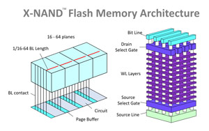
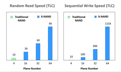
X-NAND architecture is revolutionary design architecture to eliminate this limitation. X-NAND architecture uses special circuit design and operation to reduce the number of page buffers for each page to only 1KB – 4KB. This allows the array to be divided into more planes to allow 4 - 16X of pages to be read and write in parallel thereby increasing the speed. Besides, it also decreases the 'bit line' length to 1/4 – 1/16. This, in turn, will reduce the data read time to about the same factor. As a result, X-NAND increases the random read and write speed by three times, sequential write speeds by 15 times, and sequentially read speed by 30 times.
Also, the X-NAND architecture can be implemented in NAND flash memory inside SSD for cloud and data centers and all levels of data storage hierarchical system from the upstream to the downstream. It can also be implemented in existing NAND flash memory technology without requiring any change in the manufacturing process. It also requires the same or smaller chip size, thus reducing the chip cost. To sum up, X-NAND provides a perfect solution for high-density, high-speed, and low-cost solutions for the next generation of NAND flash memory products.
Q. That's not all NEO Semiconductor does. What are its other focus areas?
We are currently optimizing the X-NAND architecture for embedded systems such as AI and IoT devices. For these applications, the NAND flash memory stores the data and the program code for the AI algorithm. Therefore, low data latency is extremely important for executing the program.
Besides, we plan to extend the application for X-NAND architecture to storage class memory (SCM) based on SLC or MLC NAND flash memory. This can provide a low-cost and high-speed buffer for SSD to further enhance the overall system performance.
Q. In what industries are your clients? Can you provide us with one or two success stories describing the challenges your clients faced and how your solutions helped them overcome those challenges?
Our potential customers are the NAND flash memory manufacturers or foundries. Since our debut of the X-NAND technology at the Flash Memory Summit conference at the end of 2020, we are seeking cooperation with these companies.
Our X-NAND architecture is a new design solution based on the existing 3D NAND flash memory technology. The foundries do not need to change the manufacturing process. The only change is the chip's design architecture and the layout. Therefore, X-NAND can be implemented in the next product in a shorter time. Usually, changing the process technology will take 5-10 years of development and multiple-ten billion dollars investment. X-NAND solution greatly reduces the development time, cost, and risk.
Our business model provides advanced technology IP licenses to top-tier foundries and companies. In this way, we can focus on our R&D strength and let other companies handle the manufacturing and sales. This cooperation creates a win-win solution for both our company and our customers.
Q. From your perspective, how is the industry you serve currently evolving? And what are the trends in the different categories?
NAND flash memory is the mainstream technology for the data storage industry. Its current market size is about $60 billion per year and is projected to grow to more than $80 billion in 2025. From 2014, the process technology of NAND flash memory has been switched from 2D to the 3D array. The memory array is built like a skyscraper. The memory capacity is increased by stacking more layers of memory cells rather than shrinking the memory cell size. This eliminated the bottleneck of the 2D process technology.
Moreover, NAND flash memory used 'multiple-level cells' to store more than one bit of data into a memory cell to increase the capacity. Today it can store 3-4 bits data, called TLC (triple-level cell) and QLC (quad-level cell). The current capacity for NAND flash memory has reached one terra bits (1TB) per chip. The density will be continuously increased in the future.
On the other hand, more layers and more levels of data stored in the cells lead to slower data read and write speeds. This degraded performance development trend is against the industry's requirement, especially for the high-speed 5G and AI applications. This problem needs to be solved urgently. Our X-NAND is targeted to address this problem.
Q. What new endeavors is your company currently undertaking?
Besides X-NAND technology, we are developing several new technologies for the next generation of 3D emerging memories. Our goal is to increase their performance and capacity and reduce the cost. We will announce these technologies soon.
Q. What do you think are the biggest challenges your industry will face in the next five years?
The biggest challenge for the data storage industry in the next five years is the speed requirement, especially for the booming 5G, AI, and IoT applications. These applications require transferring and processing massive data at extremely high speed, which the traditional NAND flash memory cannot fulfill. Especially each next generation of NAND flash memory will become 2-4 times slower; the slow speed of NAND flash has become the bottleneck for future technology development.
The slow speed of NAND flash memory will affect the acceptance when the industry migrates to the next generation high-speed interfaces, such as 6G and 7G spectrum of mobile phones, PCIe 5.0 and 6.0 of the computer peripheral interfaces, and other ultra-high-speed interfaces such as CXL and N-link, and so on. The current solution is to add an extra layer in the memory hierarchy called storage class memory (SCM) between DRAM and NAND flash memory. However, these memories are costly. Therefore, the speed issue of the NAND flash memory needs to be addressed as soon as possible for the coming AI and IoT era.
Q. What plans for transformation are you pursuing to remain relevant now and in the future?
Our ultimate goal is to promote our technology to top-tier NAND flash memory companies. Also, we aim to implement X-NAND to all levels of data storage markets. In addition to X-NAND, we have developed several advanced technologies in other fields. We will announce these technologies in the near future. I hope NEO Semiconductor will become an IP provider for many wonderful technologies for our world in the future.
Q. What is your final message to The Silicon Review readers and to your current and future customers and partners?
We are currently at the coming edge of a new era for ML, AI, and IoT technology. The semiconductor developments since the past decades allow big-data computing and ultra-fast communication to come true. More real-time AI-assistant applications will soon dominate our everyday tasks and make our life more convenient. However, all the big data are stored in 40-year old NAND flash memory technology. We are very proud that the X-NAND architecture re-innovates the NAND flash memory to address the high-speed requirement. We believe X-NAND will start a revolution for the speed of the data storage industry!
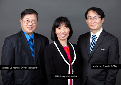
Leadership | NEO SEMICONDUCTOR
Andy Hsu is the founder and Chief Executive Officer of NEO SEMICONDUCTOR. He is an inventor of more than 120 U.S. patents. He has over 25 years of experience in leading R&D team and Engineering team to develop more than 60 memory products. He earned a MS degree in Electrical, Computer, and System Engineering (ECSE) from Rensselaer Polytechnic Institute (RPI) and a BS degree from National Cheng-Kung University in Taiwan.
Ray Tsay, co-founder, is the VP (Engineering) of NEO SEMICONDUCTOR. He has over 30 years of experience in semiconductor industry. He holds a MS degree in Electrical and Computer Engineering from Arizona State University and a MS degree in Chemical and Material Engineering from University of Iowa.
Miki Huang is the co-founder of NEO SEMICONDUCTOR. She has 19 years of IT experience in the semiconductor, pharmaceutical, and medical device industries. She earned a MS in Environmental Health from SUNY Albany and a PhD degree in Environmental and Industrial Health from University of Michigan.
“X-NAND increases the random read and write speed by three times, sequential write speeds by 15 times, and sequentially read speed by 30 times.”
MOST VIEWED ARTICLES
RECOMMENDED NEWS


TOP NEWS
YOU MAY ALSO LIKE