50 Most Trustworthy Companies of the Year 2021
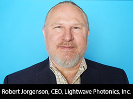
‘Our Primary Focus is on Revamping the Entire Spectrum of the MicroLED Market’: Robert Jorgenson, CEO of Lightwave Photonics, Inc.
The Silicon Review
“If customers don’t have the downstream processes, we can arrange to have MicroLEDs with our mirrors made for them.”
Over the last decade, the Light-Emitting Diodes (LEDs) industry has experienced tremendous growth and change, with new applications, increasing efficiencies, and lower costs throughout. We have witnessed a disruptive change that has made any previous technology obsolete. The LED will move forward and, within lighting technology, contribute to energy conservation, and conventional light sources will survive in small niches.
Lightwave Photonics, Inc. (LPI) is a materials technology company developing advanced technology for the large and expanding market in Light-Emitting Diodes (LEDs). LPI’s nitride materials innovations, crystal growth know-how, and patented LED structures have the potential to dramatically improve the efficiency of LEDs, obtaining more lumens of visible light per watt while reducing production costs. Lightwave Photonics, Inc. was founded in 2007 and is headquartered in Saint Paul, MN.
To highlight and further understand what Lightwave Photonics, Inc. stands for and seeks to explore in this segment, I sat down with Robert Jorgenson, who serves as the company’s Chief Executive Officer.
Below is an excerpt
Q. As a journalist, I find Lightwave Photonics quite striking. From the emotional branding standpoint, it has that appeal. How did you come up with the brand name?
A friend of the company originally proposed the name. The name is fitting because of the ongoing discussion about whether light is a wave or a particle. When things get small, light acts as a wave. When things are big, light acts as a particle. Since we are unique in that we use small vertical geometries to optimize the performance of our LEDs, it makes sense that we call ourselves light-wave photonics as opposed to light-particle photonics.
Q. Brief us about your company’s journey so far.
LPI began as a typical garage startup… but what was ironic about LPI was we didn’t have a garage. It’s funny now, but it was also painfully true at the time. Essentially, the company started with my patent for mirrors that can be used as the template for the subsequent growth of crystalline LEDs. All LEDs except for OLEDs are crystalline, by the way. That led to a small investment. With the small investment, we spent most of our funds on renting equipment at a University user lab to make our first mirrors. From the literature, it was clear that the materials would be compatible with the layered crystal stack growth, but it’s nice to have something to show your future customers. The work was very successful, but University labs are not great for repeatability or keeping confidential information.
Then with some small contracts, we were able to get a garage-like space and start pulling in our own equipment from used equipment sources. It wasn’t ideal at the time because all we could afford was sputtering equipment. Sputtering is the process whereby atoms are ejected from a target or source material that is to be deposited on a substrate. It’s very inexpensive. Our challenge was to use this equipment to make crystalline materials. To make these crystalline materials, the rest of the industry used MOCVD (metal organic chemical vapor deposition). This technology is used to deposit very thin layers of atoms onto a semiconductor wafer. MOCVD is the workhorse of the LED industry. It’s very good at growing crystalline materials, but it was prohibitively expensive for a real startup like ours. It’s amazing how expensive MOCVD equipment is, and the cost of the chemicals to run the system is equally amazing—for a startup, sputtering costs about five percent the cost of MOCVD when you consider everything.
With the used sputtering equipment, we were able to duplicate the materials we produced at the university labs and make some significant technology advancements. But, by the time that we had everything up and running (eight years ago), the industry had changed. The brute force methods of making LEDs efficient had dominated the industry infrastructure so much that our inexpensive elegant wave optics approach couldn’t get the attention. Our potential customers couldn’t hear us over the noise of all the money they were making.
Today, MicroLEDs are expected to double the LED industry, but the standard tricks like patterned sapphire substrates for making LEDs bright do not work for smaller MicroLEDs. Those traditional designs use pattern feature sizes that are just too big for MicroLEDs. Our cermet mirrors sit very close, directly under the LED crystal, as a crystal growth template to allow our superior wave optics. It’s been a long road, but it’s good that we stuck with it.
Also, LPI has many firsts:
- First to commercialize the growth of nitride semiconductors on metals (cermets),
- First to commercialize low-temperature epitaxial growth by sputtering of gallium nitride-based compound semiconductors,
- First to create metal (cermet) semiconductor multilayer mirrors.
Q. What can you tell us about the different products Lightwave Photonics offers for MicroLEDs?
To start customers off, we supply single-layer mirrors so that they can dial in their processes. Once they get past that stage, we provide more reflective multilayer mirrors. These mirrors can be optimized for red, green, or blue light emitters. We also have mirrors that can cover the entire visible spectrum. If customers don’t have the downstream processes, we can arrange to have MicroLEDs with our mirrors made for them.
Q. How do your products help customers achieve sub-micron optical cavity thickness, improved device performance, and reduced manufacturing cost?
When customers have our template for growing subsequent crystalline LED layers, there are certain benefits that they don’t otherwise have. First, they don’t have to use their expensive MOCVD systems to grow thick buffer layers upon other substrates, which cuts their MOCVD cycle time in half. Since our templates are reflective, the distance of the active layers to our mirrors is controlled by the customer, where the active layer can be positioned in the sweet spot for optimal light output. The light produced in the active region constructively resonates with the light reflected from our mirrors, enhancing the light emission to the top of the device. It’s very eloquent.
Q. That’s not all Lightwave Photonics does. What are its other focus areas?
Since our sputtering Gallium Nitride (GaN) based LEDs growth is performed at such a low temperature, growing highly doped GaN for ohmic contacts in power electronics is interesting. For such a customer, we are open to providing our processes and associated equipment (through an OEM partner) with a license.
Q. About the future, where do you see Lightwave Photonics a couple of years from now?
While LPI’s focus is on revamping the entire spectrum of the MicroLED market, MicroCavity MicroLED’s have the potential to change the face of the augmented reality market. Augmented reality glasses (A/R) need a solid solution for their devices to work correctly in a non-bulky way. They require reliable manufacturing processes where beam shaping is a big concern to ensure light emission from the top surface of the MicroLED and allowing the light to form a narrow beam like a projector. LPI’s technology solves this problem without the use of lenses or mirrors. In addition, these solution displays use fewer MicroLEDs that in turn play a vital role in reducing the price of MicroLED displays.
“LPI was the first company to commercialize the growth of nitride semiconductors on metals (cermets) and low-temperature epitaxial growth by sputtering of gallium nitride-based compound semiconductors.”
MOST VIEWED ARTICLES
RECOMMENDED NEWS


TOP NEWS
YOU MAY ALSO LIKE


_2025-11-17_06-38-14.webp)