>>
Industry>>
Supply chain management>>
Why the Semiconductor Supply C...Why the Semiconductor Supply Chain Depends on Specialized Materials
The Silicon Review
18 August, 2026
Author:
The Silicon Review Team
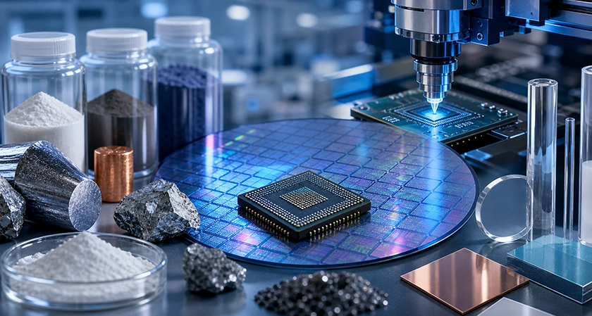
Discussions about semiconductor manufacturing often focus heavily on chip designers, multi-billion-dollar fabrication facilities, and advanced lithography equipment. However, this perspective overlooks a hidden reality: every modern fab relies on a highly specialized network of upstream materials suppliers. Before they can enter a cleanroom, silicon wafers, ultra-pure chemicals, specialty gases, and deposition materials must meet remarkably demanding specifications. At these nanoscopic scales, a factory is not a self-contained unit. Ultimately, semiconductor supply-chain resilience depends not only on expanding physical manufacturing capacity but also on securing reliable, continuous access to this specialized ecosystem of upstream materials.
Why Semiconductor Manufacturing Requires So Many Specialized Materials
Wafer fabrication is not a single production process, but rather a sequence of hundreds of highly sensitive manufacturing stages. A typical semiconductor passes through multiple complex operations over several months, including thin-film deposition, photolithography, wet and dry etching, surface cleaning, ion implantation, and chemical-mechanical polishing.
Because these stages are highly interdependent and many are repeated throughout the process, different steps demand distinct semiconductor materials with tightly controlled physical and chemical properties. A photolithography stage requires specific light-sensitive polymers, while an ion implantation stage relies on precise dopant atoms accelerated in a vacuum. Fabs cannot simply substitute these inputs with ordinary industrial-grade materials. At nanoscopic scales, even small amounts of contamination or process variation can create defects and reduce manufacturing yield. Consequently, the steady flow of specialized semiconductor manufacturing materials—even in relatively small quantities—is a production-critical requirement for uninterrupted facility operations.
Where Specialized Materials Enter the Chip Manufacturing Process
Wafers and Substrate Materials
Silicon wafers serve as the foundational substrate for the vast majority of modern semiconductor devices due to silicon's useful electrical and mechanical properties and its ability to be precisely doped. Depending on the application, other semiconductor materials may be required—for example, silicon carbide (SiC) for many high-voltage power applications and gallium arsenide (GaAs) for certain RF and optoelectronic devices. Whether silicon or compound semiconductor, fabrication-grade substrates demand extremely high purity, strong crystal quality, and tight dimensional consistency to support reliable manufacturing.
Specialty Chemicals and Process Gases
Wafer fabrication depends heavily on a continuous supply of highly controlled chemicals and gases. Manufacturing stages like etching, cleaning, and photolithography require distinct chemical inputs, such as the ammonium hydroxide and hydrogen peroxide mixtures used for wet cleaning, or the specialized gas mixtures used in DUV excimer light sources, in which neon can be a major consumable.
Purity and consistency matter profoundly in these applications because contamination at the semiconductor scale can lower manufacturing yield and compromise device performance. Many critical inputs therefore require semiconductor-grade purification, contamination control, qualification, and specialized handling beyond ordinary industrial specifications.
Thin-Film Deposition Materials
Throughout the manufacturing cycle, semiconductor devices are built through the repeated deposition of extremely thin layers of conductive, barrier, insulating, and other functional materials. One of the primary methods used to create these precise thin films is physical vapor deposition (PVD). During a sputtering-based PVD process, source material is physically removed from a target in a vacuum and deposited onto the substrate.
This source material must be manufactured in a highly specific form to fit the deposition system. For example, high-purity sputtering targets provide the source materials used in sputter-based PVD processes. Characteristics such as high purity, material density, controlled grain structure, alloy composition, and strict trace-element limits can affect deposition consistency, defectivity, film composition, and other resulting film properties. This level of precise material engineering exemplifies the specialized, fab-ready inputs required for modern semiconductor manufacturing.
Why Purity Turns Common Elements Into Specialized Products
The critical difference between a commercially available raw material and one prepared for a fab lies in its extreme purity requirements. A material may begin as a relatively common elemental metal or industrial gas, but it requires extensive refining, processing, and testing before it enters a cleanroom. Semiconductor-grade specifications often demand ultra-high purity levels, restricting trace-element contaminants to parts-per-million (ppm) or even parts-per-billion (ppb) thresholds.
Beyond elemental purity, specialized inputs require controlled physical properties. For example, sputtering materials must maintain a specific microstructure and density, while process chemicals require rigorous filtration and contamination control. This creates a market where batch consistency and manufacturing traceability are paramount.
Suppliers may provide lot-specific Certificates of Analysis and other quality documentation covering parameters such as purity, trace contaminants, or particle levels, depending on the material and specification. These rigorous requirements transform widely available elements into highly engineered products, creating a narrowly specialized supplier market.
Why Specialized Materials Become Supply-Chain Bottlenecks
The hyper-specialization of semiconductor inputs can create significant vulnerabilities upstream from the fab. These materials become supply-chain bottlenecks for several fundamental reasons.
First, some critical inputs are dependent on other industrial production streams. Gallium, for example, is largely recovered as a by-product of processing bauxite or zinc ores, while neon is recovered and purified through large-scale air-separation operations. Geographic concentration can further increase supply risk when production or processing capacity is clustered in a small number of regions.
Second, there are limited numbers of qualified suppliers globally capable of meeting ultra-high-purity manufacturing standards for certain materials.
Third, producing these inputs can involve specialized manufacturing capabilities and long processing timelines. Simply finding another geographical source of a raw element does not instantly solve a shortage. A replacement supplier must still meet strict trace-element specifications and undergo rigorous, time-consuming customer qualification processes before its materials can enter active production. Because fabs may have limited ability to switch materials or suppliers quickly without risking yield, these specialized constraints make semiconductor supply chains structurally vulnerable.
The Business Impact of a Small but Critical Input
From a business and operations perspective, the financial asymmetry of the materials supply chain is striking. Specialized materials may represent only a small fraction of the total investment required to build and operate a multi-billion-dollar fabrication facility. Yet the absence of a single specialized gas, chemical, or deposition material can still disrupt that large capital investment.
A missing or unqualified material can cause production interruptions, delay wafer processing, and reduce manufacturing utilization. Because semiconductor production involves tightly interconnected and time-sensitive process flows, disruptions can translate into delayed customer orders and weaker capital efficiency.
Sudden material shortages can also force procurement teams to accelerate alternate-supplier qualification and increase inventory pressure. Ultimately, the economic purchase cost of a specialized material can be far smaller than its strategic value to production continuity and its role in reducing supply-chain and geopolitical exposure.
How Semiconductor Companies Can Build More Resilient Material Supply Chains
To mitigate materials-related supply risks, semiconductor companies can adopt resilience strategies that go beyond efficiency-only sourcing models. These strategies can include qualifying secondary suppliers where feasible, improving sub-tier visibility, regionalizing selected sources, and maintaining appropriate safety inventories for suitable high-risk materials.
Organizations should also improve supply-chain visibility deep into sub-tier vendors to monitor potential geographical bottlenecks and identify dependencies that may not be obvious at the direct-supplier level. For highly specialized, difficult-to-source materials with long lead times, inventory buffers may help bridge disruption gaps when storage, shelf life, and material characteristics allow.
Finally, buyers can develop closer relationships with specialist suppliers, continuously evaluating both their manufacturing capacity and the rigor of their quality systems. Resilience requires deliberate structural redundancy where practical rather than simply selecting the lowest-cost vendor.
Next Steps for Building a More Resilient Semiconductor Materials Strategy
Semiconductor manufacturers and supply-chain teams can take the following steps:
-
Identify the specific materials that could halt production if unavailable.
-
Map where those essential materials are processed and manufactured.
-
Determine which critical inputs rely on a single qualified supplier or region.
-
Begin qualifying alternate sources before physical disruptions occur where feasible.
-
Review safety-inventory strategies for long-lead-time specialized materials where appropriate.
True semiconductor resilience requires extending visibility far beyond fabs and equipment suppliers, reaching deep into the specialized materials ecosystem that keeps production running.






















Comments